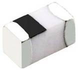
| Multilayer Chip Inductor��CL Series |
| |
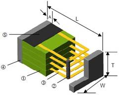
��Construction |
|
��Features
��A ceramic material construction for high frequency application up to 10GHz
��Tight tolerance physical dimensions(+/-0.05mm)
��Tight inductance tolerance and excellent Qvalue
��Available in three compact sizes of 0201,0402, 0603
��Applications
��High Frequency Application
��Cellular Phone
��EMI Countermeasure in High Frequency Circuits and Computer Communication etc.
��WLAN and RF module |
�� |
Ceramic Material |
�� |
Inner Electrode(Ag) |
�� |
Direction Mark |
�� |
Through Hole |
�� |
End-termination (Ag/Ni/Sn) |
��
|
|
��Dimensions
| Type |
Size
(Inch) |
L |
W |
T
|
A
(min./max.) |
Weight
(g)
1000pcs) |
| CL01 |
0201 |
0.6��0.03 |
0.3��0.03 |
0.33max. |
0.1/0.2 |
0.28 |
| CL02 |
0402 |
1.0��0.10 |
0.5��0.10 |
0.5��0.10 |
0.1/0.3 |
0.98 |
| CL03 |
0603 |
1.6��0.15 |
0.8��0.15 |
0.8��0.15 |
0.2/0.3 |
3.47 |
|
��Part Numbering
|
|
|
|
|
|
|
|
|
|
|
Dimensions |
01:0201
02:0402
03:0603 |
|
Inductance
Tolerance |
| J:��5%
K:��10%
S:��0.3nH |
|
Packaging
Code |
| T:Taping Reel |
|
Inductance |
1N0:1.0nH
39N:39nH
R10:100nH |
|
| |
|
|
|
|
| |
|
|
|
|
|
| |
��Electrical Specifications
CL01 Multilayer Chip Inductors Type
Inductance
(nH) |
Tolerance |
Quality
Factor
min. |
L/Q
Freq.
(MHz) |
Q (Typical)
Freq. (MHz) |
SRF
(GHz) min. |
DCR
(��) max. |
IDC
(mA) max. |
100 |
500 |
800 |
0.3 |
��0.3nH |
4 |
100 |
5 |
13 |
18 |
10 |
0.07 |
250 |
0.4 |
��0.3nH |
4 |
100 |
5 |
13 |
18 |
10 |
0.07 |
250 |
0.5 |
��0.3nH |
4 |
100 |
5 |
13 |
18 |
10 |
0.08 |
250 |
0.6 |
��0.3nH |
4 |
100 |
5 |
13 |
18 |
10 |
0.08 |
250 |
0.7 |
��0.3nH |
4 |
100 |
5 |
13 |
18 |
10 |
0.09 |
250 |
0.8 |
��0.3nH |
4 |
100 |
5 |
13 |
18 |
10 |
0.10 |
250 |
0.9 |
��0.3nH |
4 |
100 |
5 |
13 |
18 |
10 |
0.10 |
250 |
1 |
��0.3nH |
4 |
100 |
5 |
15 |
19 |
10 |
0.14 |
250 |
1.1 |
��0.3nH |
4 |
100 |
5 |
15 |
19 |
10 |
0.14 |
250 |
1.2 |
��0.3nH |
4 |
100 |
6 |
15 |
20 |
10 |
0.14 |
250 |
1.3 |
��0.3nH |
4 |
100 |
6 |
15 |
20 |
10 |
0.14 |
250 |
1.5 |
��0.3nH |
4 |
100 |
6 |
15 |
20 |
10 |
0.18 |
230 |
1.6 |
��0.3nH |
4 |
100 |
6 |
15 |
20 |
10 |
0.18 |
230 |
1.8 |
��0.3nH |
4 |
100 |
6 |
15 |
20 |
10 |
0.19 |
200 |
2 |
��0.3nH |
4 |
100 |
6 |
15 |
20 |
8.8 |
0.20 |
200 |
2.2 |
��0.3nH |
4 |
100 |
6 |
15 |
20 |
8.8 |
0.22 |
200 |
2.4 |
��0.3nH |
4 |
100 |
6 |
15 |
20 |
8.3 |
0.24 |
200 |
2.7 |
��0.3nH |
5 |
100 |
6 |
16 |
20 |
7.7 |
0.25 |
200 |
3 |
��0.3nH |
5 |
100 |
6 |
16 |
20 |
7.2 |
0.28 |
180 |
3.3 |
��0.3nH |
5 |
100 |
6 |
16 |
20 |
6.7 |
0.30 |
180 |
CL01 Multilayer Chip Inductors Type
Inductance
(nH) |
Tolerance |
Quality
Factor
min. |
L/Q
Freq.
(MHz) |
Q (Typical)
Freq. (MHz) |
SRF
(GHz) min. |
DCR
(��) max. |
IDC
(mA) max. |
100 |
500 |
800 |
3.6 |
��0.3nH |
5 |
100 |
6 |
16 |
20 |
6.4 |
0.30 |
170 |
3.9 |
��0.3nH |
5 |
100 |
7 |
16 |
20 |
6.0 |
0.30 |
170 |
4.3 |
��0.3nH |
5 |
100 |
7 |
16 |
20 |
5.7 |
0.40 |
150 |
4.7 |
��0.3nH |
5 |
100 |
7 |
16 |
20 |
5.3 |
0.40 |
150 |
5.1 |
��0.3nH |
5 |
100 |
7 |
16 |
20 |
5.0 |
0.40 |
150 |
5.6 |
��0.3nH |
5 |
100 |
7 |
16 |
20 |
4.2 |
0.40 |
150 |
6.2 |
��5% |
5 |
100 |
7 |
16 |
20 |
3.8 |
0.44 |
150 |
6.8 |
��5% |
5 |
100 |
7 |
16 |
20 |
3.5 |
0.50 |
150 |
7.5 |
��5% |
5 |
100 |
7 |
15 |
20 |
3.3 |
0.53 |
150 |
8.2 |
��5% |
5 |
100 |
7 |
15 |
20 |
3.2 |
0.55 |
150 |
9.1 |
��5% |
5 |
100 |
7 |
15 |
20 |
3.0 |
0.62 |
150 |
10 |
��5% |
5 |
100 |
7 |
15 |
19 |
2.8 |
0.65 |
150 |
12 |
��5% |
5 |
100 |
7 |
14 |
18 |
2.4 |
0.70 |
100 |
15 |
��5% |
5 |
100 |
7 |
14 |
18 |
2.2 |
0.80 |
100 |
18 |
��5% |
5 |
100 |
7 |
14 |
18 |
2.1 |
0.90 |
100 |
22 |
��5% |
5 |
100 |
7 |
14 |
18 |
1.8 |
1.20 |
100 |
27 |
��5% |
4 |
100 |
6 |
13 |
16 |
1.8 |
1.80 |
50 |
33 |
��5% |
4 |
100 |
6 |
12 |
14 |
1.7 |
2.10 |
50 |
39 |
��5% |
4 |
100 |
6 |
12 |
14 |
1.5 |
2.40 |
50 |
47 |
��5% |
4 |
100 |
6 |
11 |
13 |
1.3 |
2.80 |
50 |
56 |
��5% |
4 |
100 |
6 |
11 |
12 |
1.1 |
3.00 |
50 |
CL02 Multilayer Chip Inductors Type
Inductance
(nH)�� |
Tolerance |
Quality
Factor
min. |
��L/Q
Freq.
(MHz) |
Q (Typical)
Freq. (MHz) |
SRF
(GHz) min.�� |
DCR
(��) max.�� |
IDC
(mA) max.�� |
| 100 |
500 |
800 |
900 |
1800 |
2000 |
2400 |
| 1 |
��0.3nH |
8 |
100 |
9 |
25 |
34 |
36 |
57 |
63 |
73 |
10.0 |
0.12 |
300 |
| 1.1 |
��0.3nH |
8 |
100 |
9 |
25 |
34 |
36 |
57 |
63 |
73 |
10.0 |
0.12 |
300 |
| 1.2 |
��0.3nH |
8 |
100 |
11 |
28 |
37 |
40 |
63 |
70 |
82 |
10.0 |
0.12 |
300 |
| 1.3 |
��0.3nH |
8 |
100 |
11 |
29 |
39 |
42 |
65 |
73 |
85 |
10.0 |
0.13 |
300 |
| 1.5 |
��0.3nH |
8 |
100 |
11 |
27 |
35 |
38 |
38 |
65 |
75 |
6.00 |
0.13 |
300 |
| 1.6 |
��0.3nH |
8 |
100 |
11 |
30 |
39 |
42 |
64 |
71 |
81 |
6.00 |
0.14 |
300 |
| 1.8 |
��0.3nH |
8 |
100 |
11 |
28 |
36 |
40 |
57 |
61 |
73 |
6.00 |
0.14 |
300 |
| 2 |
��0.3nH |
8 |
100 |
11 |
26 |
34 |
37 |
55 |
61 |
68 |
6.00 |
0.16 |
300 |
| 2.2 |
��0.3nH |
8 |
100 |
10 |
23 |
30 |
32 |
48 |
52 |
61 |
6.00 |
0.16 |
300 |
| 2.4 |
��0.3nH |
8 |
100 |
10 |
24 |
30 |
33 |
48 |
52 |
61 |
6.00 |
0.17 |
300 |
| 2.7 |
��0.3nH |
8 |
100 |
12 |
29 |
38 |
42 |
42 |
67 |
74 |
6.00 |
0.17 |
300 |
| 3 |
��0.3nH |
8 |
100 |
11 |
27 |
34 |
37 |
53 |
58 |
67 |
6.00 |
0.19 |
300 |
| 3.3 |
��0.3nH,��10% |
8 |
100 |
10 |
25 |
32 |
34 |
49 |
52 |
60 |
6.00 |
0.19 |
300 |
| 3.6 |
��0.3nH,��10% |
8 |
100 |
10 |
23 |
30 |
32 |
46 |
50 |
56 |
5.00 |
0.22 |
300 |
| 3.9 |
��0.3nH,��10% |
8 |
100 |
11 |
26 |
33 |
35 |
50 |
54 |
61 |
4.00 |
0.22 |
300 |
| 4.3 |
��0.3nH,��10% |
8 |
100 |
10 |
23 |
29 |
31 |
43 |
46 |
50 |
4.00 |
0.24 |
300 |
| 4.7 |
��0.3nH,��10% |
8 |
100 |
10 |
23 |
30 |
33 |
46 |
49 |
55 |
4.00 |
0.24 |
300 |
| 5.1 |
��0.3nH,��10% |
8 |
100 |
11 |
25 |
32 |
35 |
47 |
49 |
52 |
4.00 |
0.27 |
300 |
| 5.6 |
��0.3nH,��10% |
8 |
100 |
11 |
25 |
32 |
35 |
47 |
49 |
52 |
4.00 |
0.27 |
300 |
| 6.2 |
��0.3nH,��10% |
8 |
100 |
11 |
25 |
31 |
33 |
45 |
47 |
52 |
3.90 |
0.32 |
300 |
| 6.8 |
��5,��10% |
8 |
100 |
11 |
25 |
31 |
34 |
45 |
48 |
51 |
3.90 |
0.32 |
300 |
| 8.2 |
��5,��10% |
8 |
100 |
11 |
25 |
31 |
34 |
43 |
44 |
44 |
3.50 |
0.37 |
300 |
| 10 |
��5,��10% |
8 |
100 |
11 |
24 |
31 |
33 |
39 |
39 |
37 |
3.20 |
0.42 |
300 |
| 12 |
��5,��10% |
8 |
100 |
11 |
24 |
31 |
33 |
39 |
39 |
37 |
2.60 |
0.50 |
300 |
| 15 |
��5,��10% |
8 |
100 |
11 |
23 |
30 |
32 |
35 |
33 |
28 |
2.30 |
0.55 |
300 |
| 18 |
��5,��10% |
8 |
100 |
11 |
23 |
30 |
30 |
29 |
27 |
18 |
2.00 |
0.65 |
300 |
| 22 |
��5,��10% |
8 |
100 |
12 |
24 |
30 |
31 |
27 |
24 |
14 |
1.60 |
0.80 |
300 |
| 27 |
��5,��10% |
8 |
100 |
11 |
24 |
29 |
30 |
21 |
16 |
2 |
1.40 |
0.90 |
300 |
CL02 Multilayer Chip Inductors Type
Inductance
(nH) |
Tolerance |
Quality
Factor
min. |
L/Q
Freq.
(MHz) |
Q (Typical)
Freq. (MHz) |
SRF
(GHz) min. |
DCR
(��) max. |
IDC
(mA) max. |
100 |
500 |
800 |
900 |
1800 |
2000 |
2400 |
33 |
��5,��10% |
8 |
100 |
12 |
23 |
26 |
27 |
11 |
4 |
- |
1.20 |
1.00 |
200 |
39 |
��5,��10% |
8 |
100 |
11 |
22 |
24 |
24 |
1 |
- |
- |
1.10 |
1.20 |
200 |
47 |
��5,��10% |
8 |
100 |
11 |
21 |
23 |
23 |
- |
- |
- |
0.90 |
1.30 |
200 |
56 |
��5,��10% |
8 |
100 |
11 |
21 |
22 |
22 |
- |
- |
- |
0.75 |
1.40 |
200 |
68 |
��5,��10% |
8 |
100 |
12 |
21 |
21 |
19 |
- |
- |
- |
0.75 |
1.40 |
180 |
82 |
��5,��10% |
8 |
100 |
11 |
18 |
15 |
13 |
- |
- |
- |
0.60 |
1.60 |
150 |
100 |
��5,��10% |
8 |
100 |
11 |
19 |
15 |
12 |
- |
- |
- |
0.60 |
1.60 |
150 |
120 |
��5,��10% |
8 |
100 |
11 |
15 |
7 |
2 |
- |
- |
- |
0.60 |
1.60 |
150 |
150 |
��5,��10% |
8 |
100 |
12 |
18 |
9 |
4 |
- |
- |
- |
0.55 |
2.40 |
140 |
CL03 Multilayer Chip Inductors Type
Inductance
(nH) |
Inductance
Tolerance
(nH or %) |
Quality
Factor
min.�� |
L/Q
Freq.
(MHz) |
Q (Typical)
Freq. (MHz) |
SRF(GHz) min. |
DCR(��) max. |
IDC(mA) max. |
| 100 |
500 |
800 |
| 1 |
��0.3nH |
8 |
100 |
15 |
36 |
49 |
6.0 |
0.10 |
500 |
| 1.2 |
��0.3nH |
8 |
100 |
15 |
36 |
49 |
6.0 |
0.10 |
500 |
| 1.5 |
��0.3nH |
8 |
100 |
14 |
34 |
47 |
6.0 |
0.10 |
500 |
| 1.8 |
��0.3nH |
8 |
100 |
17 |
40 |
55 |
6.0 |
0.10 |
500 |
| 2.2 |
��0.3nH |
8 |
100 |
15 |
38 |
49 |
6.0 |
0.10 |
500 |
| 2.7 |
��0.3nH |
8 |
100 |
14 |
37 |
48 |
6.0 |
0.10 |
500 |
| 3.3 |
��0.3nH,��10% |
10 |
100 |
16 |
40 |
51 |
6.0 |
0.13 |
500 |
| 3.9 |
��0.3nH,��10% |
10 |
100 |
14 |
36 |
48 |
6.0 |
0.15 |
500 |
| 4.7 |
��0.3nH,��10% |
10 |
100 |
14 |
37 |
48 |
4.0 |
0.20 |
500 |
| 5.6 |
��0.3nH,��10% |
10 |
100 |
14 |
36 |
46 |
4.0 |
0.23 |
500 |
| 6.8 |
��5,��10% |
10 |
100 |
15 |
37 |
48 |
3.75 |
0.25 |
500 |
| 8.2 |
��5,��10% |
10 |
100 |
16 |
39 |
50 |
3.30 |
0.28 |
500 |
| 10 |
��5,��10% |
12 |
100 |
16 |
37 |
47 |
3.0 |
0.30 |
300 |
| 12 |
��5,��10% |
12 |
100 |
15 |
36 |
45 |
2.6 |
0.35 |
300 |
| 15 |
��5,��10% |
12 |
100 |
16 |
38 |
48 |
2.3 |
0.40 |
300 |
| 18 |
��5,��10% |
12 |
100 |
17 |
38 |
47 |
2.0 |
0.45 |
300 |
| 22 |
��5,��10% |
12 |
100 |
18 |
40 |
49 |
1.6 |
0.50 |
300 |
| 27 |
��5,��10% |
12 |
100 |
18 |
40 |
47 |
1.4 |
0.55 |
300 |
| 33 |
��5,��10% |
12 |
100 |
17 |
40 |
46 |
1.2 |
0.60 |
300 |
| 39 |
��5,��10% |
12 |
100 |
19 |
40 |
46 |
1.1 |
0.65 |
300 |
| 47 |
��5,��10% |
12 |
100 |
17 |
36 |
39 |
0.9 |
0.70 |
300 |
| 56 |
��5,��10% |
12 |
100 |
18 |
36 |
37 |
0.9 |
0.75 |
300 |
| 68 |
��5,��10% |
12 |
100 |
18 |
35 |
36 |
0.7 |
0.85 |
300 |
| 82 |
��5,��10% |
12 |
100 |
18 |
33 |
29 |
0.6 |
1.00 |
300 |
| 100 |
��5,��10% |
12 |
100 |
18 |
28 |
16 |
0.6 |
1.20 |
300 |
| 120 |
��5,��10% |
8 |
50 |
- |
- |
- |
0.5 |
2.30 |
250 |
| 150 |
��5,��10% |
8 |
50 |
- |
- |
- |
0.5 |
2.40 |
250 |
| 180 |
��5,��10% |
8 |
50 |
- |
- |
- |
0.4 |
2.70 |
250 |
| 220 |
��5,��10% |
8 |
50 |
- |
- |
- |
0.4 |
3.00 |
250 |
��Environmental Characteristics
Electrical Performance Test
Item |
Requirement |
TestCondition |
Inductance |
In within specified tolerance |
a. Temperature: 25��1��C
b. Relative Humidity: 45 to 85%RH
c. Atmospheric Pressure: 86 to 106kpa
d. Measuring equipment and fixture:
0201: HP4291B+Agilent16196C
0402: HP4291B+Agilent16193A
0603: HP4291B+Agilent16192A |
Q Value |
In accordance with electrical specification |
a. Temperature: 25��1��C
b. Relative Humidity: 45 to 85%RH
c. Atmospheric Pressure: 86 to 106kpa |
DC Resistance |
In accordance with electrical specification |
a. Temperature: 25��1��C
b. Relative Humidity: 45 to 85%RH
c. Atmospheric Pressure: 86 to 106kpa
d. Measuring equipment: HP 4338 |
Temperature
Characteristics |
Within specified tolerance |
a. Temperature range: -30 to��85��C
b. Reference temperature: 25��C |
Mechanical Characteristies Test
Item |
Requirement |
TestCondition |
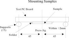
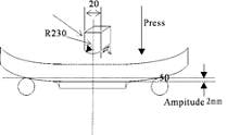
Bending Strength |
No mechanical damage shall be observed |
Solder the chip to test jig then apply a force in the direction shown in below. The soldering shall be done with the reflow method and shall be conducted with care so that the soldering is uniform and free of defects such as heat shock. |
|
|
Solderability |
More than 75% of the terminal electrode part shall be covered with fresh solder |
Immerse a test sample into a methanol solution containing rosin,preheat it at 150 to 180��C for 3 to 5 seconds and immerse into molten solder of 245��5��C for 5��0.5 seconds. |
Resistance
to Soldering Heat |
No visible damage |
Immerse a test sample into a methanol solution containing resin, preheat it at 150 to 180��C for 2 to 3 minutes and immerse into molten solder of 260��5��C for 10��0.5 seconds so that both terminal electrodes are completely submerged. |
Appearance |
In accordance with specification |
Inductors shall be visually inspected for visible evidence of defect |
Dimension |
In accordance with dimension specification |
Dimension shall be measured with caliper or micrometer |
Climatic Test
Item |
Requirement |
TestCondition |
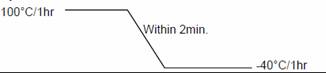
Thermal Shock |
No visible damage
Inductance variation within 10%
Q variation within 20% |
Solder a test sample to printed circuit board, and conduct 100
cycles of test under the conditions shown as below.
Cycle:
 |
|
Thermal Shock
High Humidity State Life |
No visible damage
Inductance variation within 10%
Q variation within 20% |
Keep a test sample in an atmosphere with a temperature of
70��2��C, 90~95%RH for 500��12 hours. After the test, keep the
test sample at a normal temperature for 1 to 2 hours, and then
carry out measurement. |
High Humidity Load Life |
No visible damage
Inductance variation within 10%
Q variation within 20% |
Solder a test sample to printed circuit board then keep the test
sample in an atmosphere with a temperature of 70��2��C,
90~95%RH for 500��12 hours while supplying the rated current.
After the test, keep the test sample at a normal temperature for 1
to 2 hours, and then carry out measurement. |
High Temperature State Life |
No visible damage
Inductance variation within 10%
Q variation within 20% |
Keep a test sample in an atmosphere with a temperature of
100��2��C for 500��12 hours. After the test, keep the test sample
at a normal temperature for 1 to 2 hours, and then carry out
measurement. |
High Temperature Load |
No visible damage
Inductance variation within 10%
Q variation within 20% |
Solder a test sample to printed circuit board then keep the test
sample in an atmosphere with a temperature of 100��2��C for
500��12 hours while supplying the rated current. After the test,
keep the test sample at a normal temperature for 1 to 2 hours,
and then carry out measurement. |
��Storage Temperature: 25��3��C; Humidity 80%RH
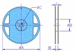
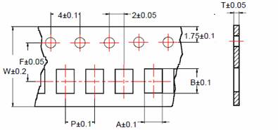
��Packaging
|